10+ dram block diagram
Code for the EVAP System Monitor. Beauchamp said CXL 20 supports switching so using a x16 link to a switch-fanout multi-slot 10 slots memory box is conceivable.

Fpgas Fpga Cpu News
N TW Timing cycle time 938ps CL 14 DDR3-2133 -093 107ns CL 13 DDR3-1866 -107 125ns CL 11 DDR3-1600 -125 15ns CL 9 DDR3.

. Part Number and Part Marking Information Part Number Ordering Micron LPDDR4 devices are available in different configurations and densities. Ie the amount of. A dynamical system may be defined formally as a measure-preserving transformation of a measure space the triplet T X Σ μ ΦHere T is a monoid usually the non-negative integers X is a set and X Σ μ is a probability space meaning that Σ is a sigma-algebra on X and μ is a finite measure on X ΣA map Φ.
X X is said to be Σ-measurable if and only if for every σ. No external DRAM or processor required for RAID operation. New thread block cluster feature exposes control of locality across multiple SMs.
Volume is a measure of occupied three-dimensional space. OFAC administers a number of different sanctions programs. This architecture is utilized by AMDs recent microarchitectures for both CPU ie Zen and graphics eg Vega and any other additional accelerators they might add in the futureThe fabric was first announced and.
All DRAM sends data in bursts packing the information into a single block and the size of the burst in todays memory is nearly always 8 bits. Refer to Package Block Diagrams section and Monolithic Device Addressing section. In February of 2017 Lisa Su AMDs CEO announced their future roadmap to include Zen 2 and later Zen 3On Investors Day May 2017 Jim Anderson AMD Senior Vice President confirmed that Zen 2 was set to utilize 7 nm processInitial details of Zen 2 and Rome were unveiled during AMDs Next Horizon event on November 6 2018.
Due to the way CRTs work this creates a small charge of. Data is lost when power is removed. From the large complement of off-chip DRAM frame buffer device memory and varying levels and types of on.
It is often quantified numerically using SI derived units such as the cubic meter and liter or by various imperial units such as the gallon quart cubic inchThe definition of length cubed is interrelated with volume. FUNCTIONAL BLOCK DIAGRAM FOR 4Mx16x4 BANKS SHOWN Integrated Silicon Solution Inc. The original Swingers site 16000 square feet of crazy golf in an office block next to the Gherkin.
Infinity Fabric IF is a proprietary system interconnect architecture that facilitates data and control transmission across all linked components. Start the engine cold. Part Number and Part Marking Information Part Number Ordering Micron LPDDR4 devices are available in different configurations and densities.
K JT 96-ball 8mm x 14mm Rev. The effect of a capacitor is known as capacitanceWhile some capacitance exists between any two electrical conductors in proximity in a circuit a capacitor is a component designed to add capacitance to a circuitThe capacitor was originally known as a. Note that this step must occur within 4-10 minutes from a cold engine startup if the drive cycle.
It was the first random-access digital storage device and was used successfully in several early computers. Static random-access memory static RAM or SRAM is a type of random-access memory RAM that uses latching circuitry flip-flop to store each bit. Kaby Lake is the first Optimization released as part of Intels PAO model.
Accelerate at part-throttle to 38-65 mph and maintain that speed for 2 minutes. A capacitor is a device that stores electrical energy in an electric fieldIt is a passive electronic component with two terminals. Intel W680 Chipset Block Diagram Some of the main features of the W680 chipset include a PCIe 40 x8 DMI link which connects the processor to the chipset for improved bandwidth over Intels.
The Williams tube works by displaying a grid of dots on a cathode-ray tube CRT. DRAM Operation To estimate the power consumption of DDR4 SDRAM it is necessary to understand the basic functionality of the device see the following figure. 1 to 2 ports SATA 3Gbs Port Multiplier RAID 0 1.
Afghanistan-Related Sanctions 02252022 Balkans-Related. SRAM is volatile memory. IAT PID from 40-100ºF this step requires a key off period of at least 8 hours.
N EF FBGA package Pb-free x16 96-ball 8mm x 14mm Rev. Shown in the left half of the diagram. A motherboard also called mainboard main circuit board mb mboard backplane board base board system board logic board only in Apple computers or mobo is the main printed circuit board PCB in general-purpose computers and other expandable systems.
The volume of a container is generally understood to be the capacity of the container. The term static differentiates SRAM from DRAM dynamic random-access memory which must be periodically refreshedSRAM is faster and more expensive than. C4 09172020 ISS ISS ISS ISS VDD DQ0 VDDQ NC DQ1 VSSQ NC DQ2 VDDQ NC DQ3.
1 to 5 ports SATA 3Gbs Port Multiplier RAID 0 1 3 5 10 JBOD CLONE. Zen 2 succeeded Zen in 2019. Now lets add in MemVerges memory machine technology.
Cannon Lake was originally set to replace Skylake as the next. So even if the single bit from one column is. Part Number and Part Marking Information Part Number Ordering Micron LPDDR4 devices are available in different configurations and densities.
Multiple servers sharing partitioning 5060 slots is also conceivable Building on this. The NVIDIA Hopper Architecture adds an optional cluster hierarchy shown in the right half of the diagram. K DA 78-ball 8mm x 105mm Rev.
It holds and allows communication between many of the crucial electronic components of a system such as the. It is system software that clusters many servers. 8Gb x8 DDR4 SDRAM Functional Block Diagram Sense amplifiers 8 64 64 64 DQS_t DQS_c Columns 0 1 and 2 Read drivers DQ70 READ FIFO and data MUX 8 Columns 0 1 and 2 3.
The Williams tube or the WilliamsKilburn tube after inventors Freddie Williams and Tom Kilburn is an early form of computer memory. Indulge in brunch at Duck Waffle any. 78-ball 8mm x 105mm Rev.
Refer to Package Block Diagrams section and Monolithic Device Addressing section. 256Mb SYNCHRONOUS DRAM IS4245S83200J IS4245S16160J 8M x 8 x 4 Banks 4M x16x4 Banks 54-pin TSOPII 54-pin TSOPII 54-ball BGA 54-ball BGA. Where is OFACs country list.
The sanctions can be either comprehensive or selective using the blocking of assets and trade restrictions to accomplish foreign policy and national security goals. The microarchitecture was developed by Intels RD center in Haifa Israel. Refer to Package Block Diagrams section and Monolithic Device Addressing section.
Kaby Lake KBL is Intels successor to Skylake an enhanced 14 nm process microarchitecture for mainstream desktops and mobile devices. To compare features and specifi-.

Memory Cell Computing Wikiwand

Is42s16400j 7tl Memory Cad Models Datasheet Features Video Faq

Types Of Ram Random Access Memory Computer Memory Memories

Cortex A76 Block Diagram Electrical Wiring Colours Block Diagram Diagram
How To Design A 4kx8 Bit Memory System By Using 1kx4 Bit Memory Chips Quora
Row Hammer Wikiwand

Using A Pcie Slot To Install Dram New Samsung Cxl Mem Expansion Module

Layerscape Ls1021a Smarc Som Iwave Systems

Dh Electronics Dhcom Stm32mp15
What Makes Memory Test Hard
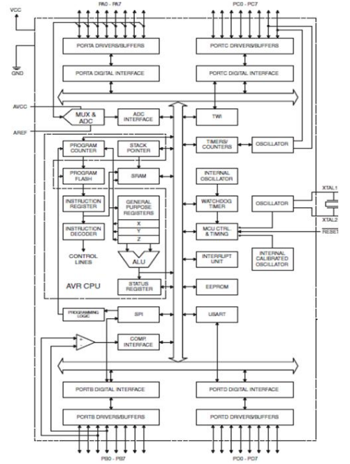
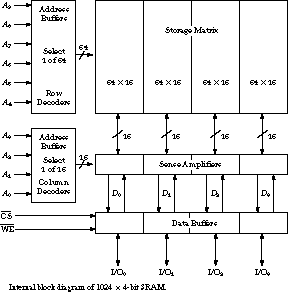
Atmega32 Memories Javatpoint

Memory Cell Computing Wikiwand

Dh Electronics Dhcom I Mx6

Click Here For Larger Imageampere S Emag 8180 Processor Block Diagram Source Ampere Ampere Block Diagram Semiconductors
What Is A Block Diagram Of An Embedded System Quora
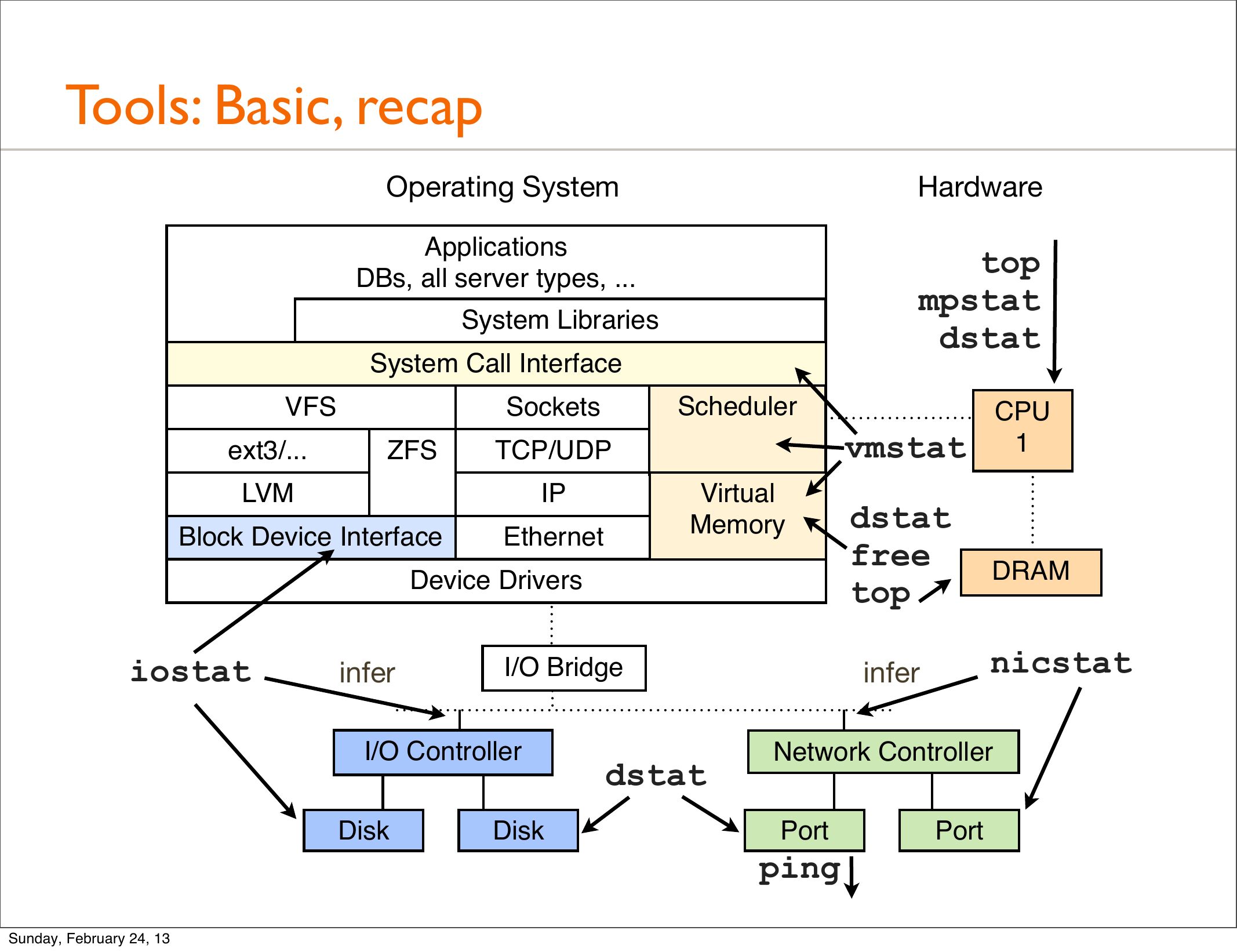
Scale Linux Performance2013 Pdf

Microarchitecture Wikiwand